for Electronic Devices (Sputtering & Ion Plating)
R&D sputtering system
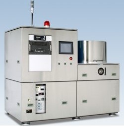
Ideal for thin film formation on irregular substrates and R & D
General Outline
This device is a sputtering device for forming a thin film on an irregular substrate.
The equipment is batch type, equipped with a magnetron cathode, and either sputter down or sputter up can be selected. In addition, substrate cleaning by reverse sputtering mechanism is also possible.
The power supply can switch between DC power supply and RF power supply.
Features / Options
- Reverse sputtering (RF) is possible by switching.
- It can be changed manually from T / S 140mm to 200mm.
- Parameters can be set for each cathode, and the four cathodes can deposit simultaneously.
- A heating mechanism compatible with a φ8 inch × 1 t quartz substrate can be attached. (Substrate surface MAX 600 °C)
Applications
Various experimental applications
For small lot production
Supports substrates such as wafers, films and molds
Specifications
- Processing method
- Batch type
- Exhaust pump
- DRP+TMP
- Installation dimensions
- W3,600㎜ × D2,500㎜ × H2,100㎜
- Equipment weight
- 2,000 kg
- Power supply capacity
- AC200V(3φ) / 36kVA(103A)
- Chamber size
- φ750㎜ × H340㎜
*For the improvement of product, please understand that the specifications are subject to change without prior notice.
**This product may be applicable to export control products such as strategic raw materials which are regulated by the Foreign Exchange and Foreign Trade Control Law.
Accordingly when you bring out the applicable products outside Japan. You should take a necessary action such as application of an export permit to the Government of Japan.